Integrated microsystems laboratory (MEMS) / Plating / Electrodeposition of metal and dielectric
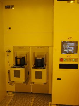
SVS Jikji-77
Supplier :
Scientific Value Solutions Corp. (SVS)
Model :
JikJi-77
Purpose :
Through Silicon Via filling of copper and Au-Sn
CAPABILITY:
Wafer size: 200 mm
Thickness range of wafers: 300 – 1200 µm
Wafer material: Silicon, Glass
Fully qualified for through silicon via AquiViaTM process under license from Alchimer, with the following modules:
- Module 1: Pre-wetting of Si wafers with 20:1 aspect ratio vias
- Module 2: Chemical grafting of 0.2-1.0 µm insulation film
- Module 3: Activation of insulation for Ni(B)
- Module 4: Electroless Ni(B) diffusion barrier
- Module 5: Cu electrofill in 50:5µm & 100:5µm TSV
- Module 6: Wafer annealing
- Module 7: 80Au/20Sn eutectic electroplating