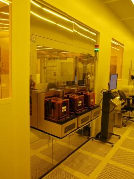
Integrated microsystems laboratory (MEMS) / Bonder / Wafer bonding
EVG Gemini 200/3
Supplier :
EV Group
Model :
GEMINI/200/3
Purpose :
Fully-automated wafer bonding for 200 mm wafers
CAPABILITY:
Processing 200 mm wafers and 3D-Integrated MEMS devices with wafer-level packages.
Bond 200 mm wafers using fusion bonding, glass frit bonding, adhesive bonding, eutectic bonding, thermo-compression bonding, transient liquid phase bonding, and solder bonding.
Wafer-to-wafer alignment accuracy: ± 0.4 µm (3 sigma)
Range of wafer thickness: 300 – 1700 µm
Temperature control: 20 – 550 °C ± 1.5%
Contact Force control: 1.5 – 100 kN ± 2%
Gas pressure control: 0.1 – 1000 mbar ± 5%
In-situ wafer treatment with formic acid vapour
Megasonic wafer cleaning

