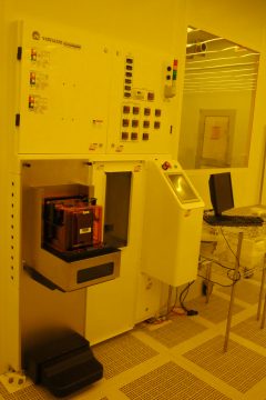
Integrated microsystems laboratory (MEMS) / Lithography / Hard Bake
Yield Engineering – YES PBV200 Vertacure
Supplier :
Yield Engineering Systems Inc.
Model :
PBV200 Vertacure
Purpose :
Anneal/Bake/Cure under controlled temperature and sub-atmospheric pressure
CAPABILITY
Wafer size: 200 mm
Production wafers per load: 50
Thickness range of wafers: 300 – 1700 µm
Temperature range: 20 – 450 °C
Pressure range: 0.1 – 500 Torr
Gases used: Oxygen, Nitrogen, Forming gas (H2 4% and N2 96%)
Wafer material: Silicon, Glass, Bonded wafers
Processes:
- Photo-resist bake processes
- Polymer curing processes
- Wafer dehydration processes
- Wafer film sublimation processes
- Glass-frit glaze cycles
- Thin film resistors thermal treatments

