Integrated microsystems laboratory (MEMS) / Metrology / Inspection visible range: particle and defect count
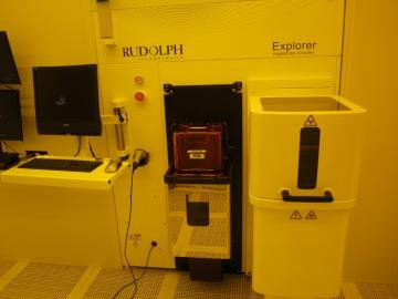
Rudolph F30-B30-E30
Supplier :
Rudolph Technologies, Inc.
Model :
F30-B30-E30
Purpose :
Automated frontside, edge and backside inspection in the visible range for 200mm wafer, and for 200 mm diced and stretched wafer on film frame.
CAPABILITY:
Wafer size: 200 mm
Thickness range of wafers: 300 – 1200 µm
Wafer types: Silicon, Glass, perforated wafers, wafers with through-silicon vias, diced wafers on film frame.
100 % front-side, edge and backside inspection
High aspect ratio through silicon via inspection
Brightfield and darkfield inspection
Resolution flexibility: 0.5 µm – 10 µm
Laser autofocus for bowed wafers
Detects blister defects, slurry, cleaning contaminants and residual films
Performs automated Edge Bead Removal metrology
Detects chips and cracks, delamination defects, backside particles, unwanted residues, scratches and defect clusters
On-the-fly defect classification and binning