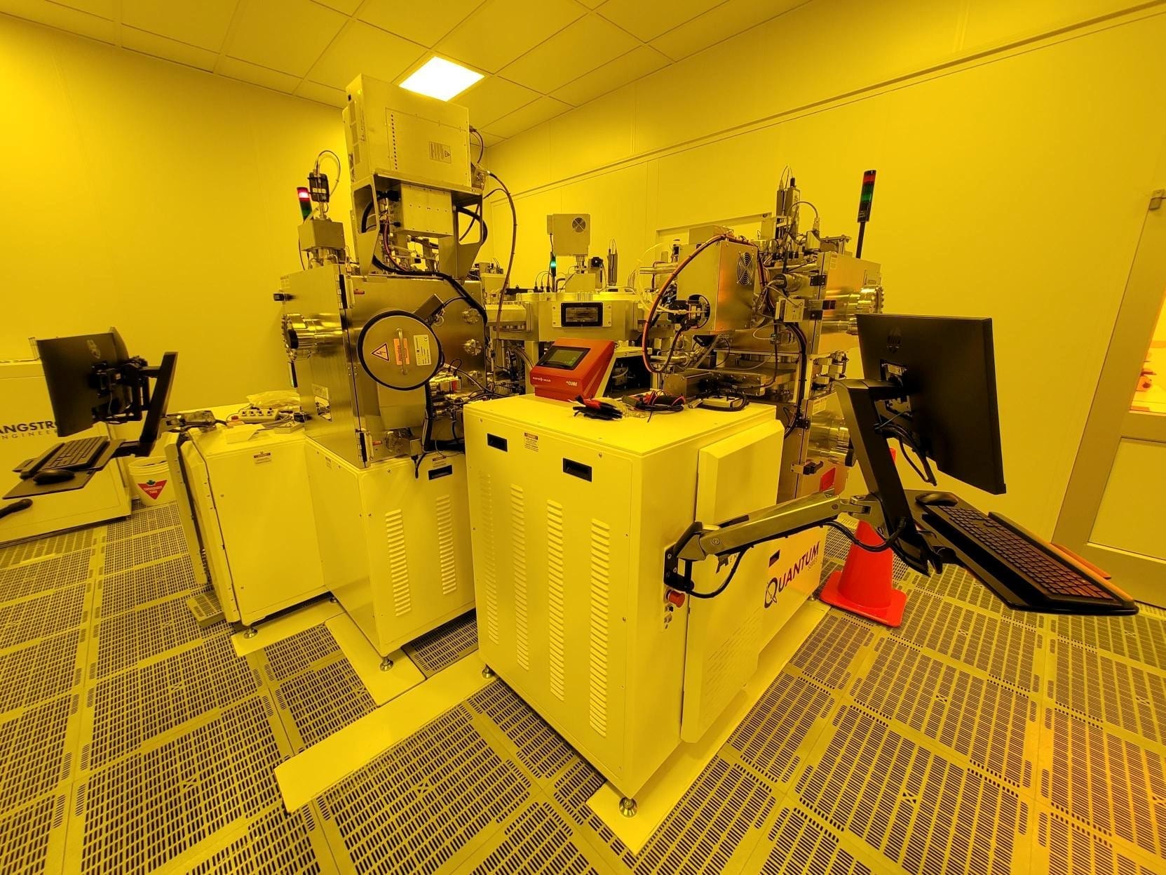
/ Quantum Device Fabrication /
Angstrom Engineering Quantum Cluster
Supplier :
Angstrom Engineering
Model :
Quantum Cluster
Purpose :
Automated multichamber superconducting-quantum material deposition platform for 200mm wafers
A fully automated 200 mm wafer (Si or Sapphire compatible) processing platform designed to support advanced quantum device fabrication using a central robotic wafer handling platform operating entirely under ultra-high vacuum (UHV) with all wafer transfers performed under continuous UHV conditions.
The tool is in a through wall configuration (Class 10 / ISO 4 environment on the wafer-facing side).
Process flows are executed across multiple chambers without breaking vacuum between steps, minimizing contamination, preserving interface quality, and ensuring highly reproducible material properties.
- UHV Sputter deposition chamber for high-quality thin films, supporting materials such as Nb, NbN, Ti, TiN, NbTiN, and Ta, widely used in superconducting and quantum device stacks (including superconducting, resonator, and quantum device applications)
- Rotating substrate stage with temperatures up to 800°C
- Supports DC, Pulsed DC, HiPIMS, and RF sputtering processes
- Reactive N₂ sputtering capability
- Two-target chamber: Simultaneous operation of two sputtering targets for co-deposition and multilayer material development
- In-situ RHEED monitoring capability
- In-situ Auger Electron Spectroscopy (AES) capability
- Dedicated UHV ion milling chamber for in-situ wafer surface preparation, cleaning, native oxide removal, and desorption processes
- Substrate temperature range from RT to 400°C
- Rotating and tilting substrate stage
- Dedicated UHV aluminum evaporation system optimized for fabrication of Al–AlOx–Al Josephson Junctions (JJ)
- Substrate temperature range from RT to 400°C
- Rotating and tilting substrate stage
- e-beam evaporator with multiple crucibles, including a dedicated Ti crucible for titanium getter operation
- Optimized for both Manhattan-style and Dolan bridge angled evaporation processes. Patented deposition compensation enables thickness non-uniformity below ±5% for Tilted evaporation on 200mm substrates.
- Integrated oxidation chamber directly above the evaporation chamber, enabling oxidation without wafer transfer or repositioning
- both dynamic and static oxidation processes optimized for in-situ AlOx Josephson Junction fabrication
- Ozone-assisted oxidation capability
- In-situ ellipsometry at wafer center with automated endpoint detection capability
- Integrated Residual Gas Analyzer (RGA) for pre-process chamber qualification and monitoring
- Secondary UHV oxidation chamber with optional high-temperature annealing capability (not operated simultaneously)
- Supports both dynamic and static oxidation processes optimized for in-situ AlOx Josephson Junction fabrication
- Ozone-assisted oxidation capability
- In-situ ellipsometry at wafer center with automated endpoint detection capability
- Integrated Residual Gas Analyzer (RGA) for pre-process chamber qualification and monitoring
- High-temperature annealing capability up to 1000°C for applications such as recrystallization, phase transformation, and crystalline structure optimization
- Fully automated platform with advanced software control and integrated in-situ metrology systems:
- Cassette handling of up to 10 wafers per automated batch
- Ellipsometry for in-situ oxidation monitoring and endpoint detection
- Quartz Crystal Microbalance (QCM) for precise metal deposition rate and thickness control
- RHEED (Reflection High-Energy Electron Diffraction) for real-time surface and crystalline structure monitoring
- Auger Electron Spectroscopy (AES) for in-process and post-process surface composition analysis