STATE-OF-THE-ART MANUFACTURING CENTER
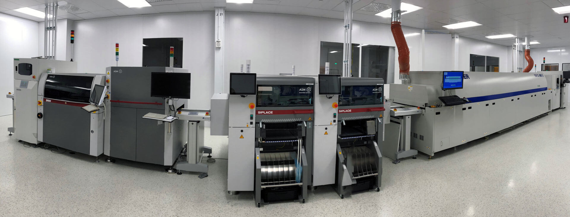
C2MI offers a wide range of equipment to help with your printed electronics or card assembly projects. True to our model of installing production-ready equipment in order to develop prototypes and processes for high volume manufacturing, we have all the necessary tools to create your circuit: from ink deposition to thermal and photonic curing, lamination and laser patterning, we can build your circuit and assemble all the parts you want to integrate. From large chips and connectors to 0102 metric components, the state-of-the-art assembly line equipped with inspection equipment is fully automated.
CARD ASSEMBLY
C2MI’s assembly line was designed with manufacturing 4.0 in mind with all inspection and control equipment integrated in the line with the placement tools and communication possibilities between them to reduce operator intervention.
Paste deposit
The first step in the on-board assembly process is paste deposition. The deposition is done with a mask printer. Fully automated, this equipment is configured to receive feedback from the ASM ProcessLens paste inspection equipment. When defects related to the printing of the chosen paste or media are seen by the inspection equipment, corrections are directly transmitted to the printer without human intervention.
Dough inspection
The ASM ProcessLens solder paste print behavior analysis system automatically learns, analyzes and optimizes print parameters.
Placement of components
The equipment on which the placement of components is done are without a doubt the most impressive in the line in terms of execution speed. The line has two ASM TX equipment that run in series and use a total of three placement heads. Components with dimensions between 0.2mmX0.1mm and 200mmX125mm can be assembled with high precision.
Automated inspection
Human eyes are often not precise enough to inspect microelectronics components. Automated optical inspection (AOI) was developed for these situations. The algorithm of the equipment makes it possible to measures real colors and dimensions on each circuit board that serve as a reference for the analysis of the electronic board. The algorithm then incorporates the varying conditions at each inspection instead of referring to learned values that may no longer be valid.
Paste
Paste inspection
Component placement
Card inspection
PRINTED ELECTRONICS
Printed electronics is an emerging technology with high growth potential because it offers lower costs, new features and capabilities. With conductive inks, it is now possible to print electronic circuits on an almost infinite variety of substrates. C2MI has adopted digital printing technologies, the most flexible to create tomorrow’s circuits.
Material deposition
The deposition of ink by jet or aerosol deposition is an emerging manufacturing technique that originated in the paper printing industry. The technique aims to deposit on a flexible substrate or other, conductive ink in a pattern of circuits that will be used to conduct current. This additive technology aims to reduce costs by depositing material only where it is needed.
Photonic curing
Photonic curing is a curing process where the ink is heated with pulsed light from a flash lamp. When ink is heated on a substrate, most of the substrate remains relatively cool because of the short exposure time (~ 1 mili second). It is then possible to reach significantly higher temperatures in the ink without damaging the substrate compared to a regular oven.
Ink jet printing
The lamination process allows for the production of multi-layered circuits for complex printed circuit boards and the application of a protective or insulating layer, as required, to previously printed circuits.
Laser patterning
The fabrication of printed electronic circuits is done in sheets comprising several units for equipment optimization and cost reduction. Since the most commonly used media in printed electronics is a flexible material, a laser is needed to cut it properly. The laser used by C2MI can also drill very small holes in various media including FR4, glass and silicon.

