
Applications field: The VSS-300 is a vacuum reflow soldering oven designed for: Reflow soldering processes with or without vacuum (up
Applications field: The VSS-300 is a vacuum reflow soldering oven designed for: Reflow soldering processes with or without vacuum (up

Applications field: Photonics: assembly of optical and photonic components (lasers, detectors, optical modules). Microelectronics: integration of semiconductors, MEMS, and hybrid

CAPABILITY : Applications field : Laser to wafer integration (III-V dies to Si photonic wafer) High accuracy die attach (Passive lense placement) Local and fast local eutectic reflow (
CAPABILITY: PCB dimensions: Single lane mode Batch mounting : L 50 × W 50 ~ L 750 × W 610
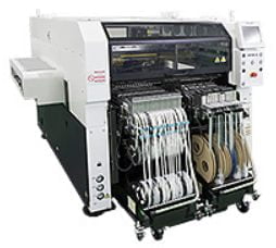
The first tool, the TX1, combines precision and high speed with a theoretical placement possibility of 48,000 components per hour