
CAPABILITY: Applications field: Wafer-level measurement of thickness, TTV, bow, and warp Optical profiler for measuring step height and CDs. Thickness
CAPABILITY: Applications field: Wafer-level measurement of thickness, TTV, bow, and warp Optical profiler for measuring step height and CDs. Thickness

Application fields: 8in wafer compression molding equipment for Fan-out wafer-level packaging (FOWLP) and heterogeneous integration Molding of reconstituted wafers (D2W)

Applications field : Wafer edge grinding Wafer terrace bevelling Wafer coring post processing of edges Specifications Fully automated mode

Applications field: The VSS-300 is a vacuum reflow soldering oven designed for: Reflow soldering processes with or without vacuum (up

Applications field: Photonics: assembly of optical and photonic components (lasers, detectors, optical modules). Microelectronics: integration of semiconductors, MEMS, and hybrid

CAPACITY: Photonic wire bond: Printing of 3D waveguide structure between optical interface (Fiber to laser, Fiber to PIC, PIC to

CAPABILITY : Applications field : Passive optical interconnexion between: Optical fibers III-V dies (Laser, SOA, Modulators, etc.. ) Si PICS (Si, SiN, TFLN Waveguides) Lens

CAPABILITY : Applications field : Laser to wafer integration (III-V dies to Si photonic wafer) High accuracy die attach (Passive lense placement) Local and fast local eutectic reflow (

CAPABILITY: APPLICATIONS FIELD: Free space optics (Active alignment) Grating coupling (Active alignment) Edge coupling (Active alignment) FLEXIBLE DEVELOPMENT WITH
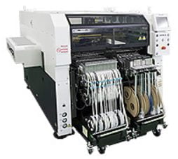
CAPABILITY: PCB dimensions: Single lane mode Batch mounting : L 50 × W 50 ~ L 750 × W 610