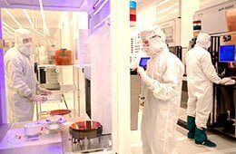
Microelectromechanical systems (MEMS) are from a technology that combines microcircuits with tiny mechanical devices such as sensors, valves, mirrors, gears, or incorporated directly triggers the semiconductor. C2MI MEMS laboratory has class 10 clean rooms and class 1 clean rooms for the wafer surface. The infrastructure is suitable for both the micro-machining surface layer and the silicon ones.
Surface micromachining
Subsurface micromachining technique is a process used to produce microelectromechanical systems (MEMS). Contrary to the bulk micromachining, where a silicon substrate is selectively etched to produce structures, surface micromachining uses microstructures by deposition and etching of the various structural layers on top of the substrate.
Generally the polysilicon is widely used as one of the layers and silicon dioxide is used as a sacrificial layer which is then removed or etched to create the necessary vacuum in the thickness. The added layers are generally very thin and sizes ranging from 2 to 5 micron.
The main advantage of this machining process is the ability to achieve monolithic microsystems in which the electronic and mechanical components are integrated in the substrate. The micro-machined component surface are smaller compared with their counterparts bulk micromachining.
Since the structures are built on top of the substrate rather than inside, the substrate properties are not as important as the bulk micromachining, and the expensive silicon wafers can be replaced by less expensive substrates, such as glass or plastic. The size of the substrates may also be much larger than a silicon wafer, and micro machining subsurface is used to produce large TFT substrates on the glass area for flat screens. This technology can also be used for the manufacture of solar cells with thin layers which can be deposited on the glass, but also on PET substrates or other non-rigid materials.
Sub-surface micromachining
Subsurface micromachining technique is a process used to produce microelectromechanical systems (MEMS). Contrary to the surface micromachining technique, which uses a thin film deposition succession and selective etching, micromachining subsurface defines structures by selectively etching the inside of a substrate. While surface micromachining creates structures over a substrate, micromachining the bulk material structures within the substrate.
Typically, silicon wafers are used as substrates for micro-machining subsurface, because they can be etched anisotropically wet forming very regular structures. Wet etching generally used alkaline liquid solvents, such as potassium hydroxide (KOH) or tetramethylammonium hydroxide (TMAH) to dissolve the silicon that has been exposed during photolithographic masking step.
These alkaline solvent dissolve silicon highly anisotropic manner with crystallographic orientations. This dissolution is up to 1000 times faster than the others. This approach is often used with very specific crystallographic orientations in the raw silicon to produce shaped grooves V. The surface of these grooves can be atomically smooth if the engraving is done correctly, and the dimensions and angles can be defined accurately.

